
Lead Advanced Microelectronics Packaging Design Engineer
Los Angeles, California; El Segundo, California Job ID JR2025445969 Category Engineering - Electronic and Electrical Role Type Onsite Post Date Jun. 10, 2025Job Description
At Boeing, we innovate and collaborate to make the world a better place. We’re committed to fostering an environment for every teammate that’s welcoming, respectful and inclusive, with great opportunity for professional growth. Find your future with us.
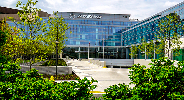
Boeing Defense Space & Security has an exciting opportunity as a Lead Advanced Microelectronics Packaging Design Engineer. Come join us as part of our Electronics Packaging team located in El Segundo, CA.
Packaging Electronics team focuses the majority of their time on Satellite missions. However, our diverse development portfolio provides opportunities to learn with exposure to the breadth of the Boeing product line – approximately half our design work is within the Space & Launch business unit, and half is from other parts of Boeing (AvionX; Missiles & Weapons; Strike, Surveillance and Mobility; and Autonomous Systems)..
Using first principals thinking, Engineers will work on electronic packaging designs and take it from cradle to grave. Working within a collaborative team environment, surrounded by world class engineers and mentors, you will design within the full life cycle and see your work from proposal all the way to delivery and production. We’re highly supportive of innovative thinking, we respect and acknowledge hard work, we recognize maturity and integrity, and we reward bottom-line achievement. At Boeing, we value your curiosity, your determination, and your imagination. #YouWillChangeTheWorld
Position Responsibilities:
Designing and optimizing layout for advanced substrates of HDI IC substrate, Silicon, or LTCC substrates, considering electrical, thermal, and mechanical requirements.
Collaborate in multi-functional discussions for package architecture and technology roadmap (partner with Silicon IC team to optimize chip Floorplan and bump placement).
Cross-functional interface with IC design, materials, SI/PI, thermal, systems, and production teams to optimize package solutions on cost, performance, manufacturability, and reliability
Interface with packaging assembly and substrate suppliers for new product bring-up, qualification and production ramp
Interface with other operations functional groups such as product engineering, foundry, test, and QA
Create and execute substrate breakout patterns for ASIC packaging
Optimize package pinouts by evaluating system-level trade-offs - Conduct package routing, placement, stack-up, reference plane, and power distribution activities
Conduct design feasibility studies to assess package design goals encompassing size, cost, and performance
Develop symbols and CAD library databases using Cadence APD or Mentor Xpedition tools
Works under minimal direction
Basic Qualifications (Required Skills/Experience):
Ability to obtain a U.S. Security Clearance
Bachelor of Science degree from an accredited course of study in engineering, engineering technology (includes manufacturing engineering technology), chemistry, physics, mathematics, data science, or computer science
5 years of experience as a substrate designer or 9+ years of professional experience with substrate layout design
Hands-on experience with package design and proficient in Cadence Allegro platform tools (PCB Editor, Advanced Package Designer, APD/SiP) or Mentor Xpedition platform tools.
Preferred Qualifications (Desired Skills/Experience):
Experience with TSV, 2D/2.5D and 3D package connection.
Hands-on expertise of advanced and new assembly processes for flipchip, wirebond, and MCM packages
SI/PI tools (XtractIM, PowerSI, HFSS, Q3D, etc.), package model extraction, S-parameters and RLGC model.
Substrate manufacturing process, structure, design rules and material property.
Solid understanding of high-speed interfaces, including DDR, PCIe, NAND, etc.
Consistent track record to drive package selection through feasibility studies and drive chip Floor planning and bump assignment.
Familiar with package design reviews and familiarity with CAM350/Valor or Calibre and CAD.
Knowledge of high-speed layout constraints (crosstalk mitigation, differential pairs, EMI/RFI, PCB/package resonance).
Familiar with Cadence Concept HDL for schematic review, experience in schematic capture and system integration.
Experience in advanced node IC layouts such as 22nm, 16nm, 7nm, 5nm or below
Experience in layout of sensitive RF blocks such as low noise amplifiers, voltage controlled oscillators and mixers
Understanding of layout considerations for device matching, coupling and noise isolation
Knowledge of advanced substrate manufacturing/process
Knowledge of failure analysis techniques on advanced node silicon products
Conceptual knowledge of package cost structure
Knowledge of GD&T and be able to read/comprehend mechanical drawings
Excellent oral and written communication skills and ability to communicate across multiple disciplines with internal and external customers
Computer proficiency and ability to use and navigate the internet and various computer software programs (e.g. Microsoft Office Suite)
Skill and ability to collect, organize, synthesize, and analyze data; summarize findings; develop conclusions and recommendations from appropriate data sources.
Drug Free Workplace:
Boeing is a Drug Free Workplace where post offer applicants and employees are subject to testing for marijuana, cocaine, opioids, amphetamines, PCP, and alcohol when criteria is met as outlined in our policies.
Total Rewards & Pay Transparency:
At Boeing, we strive to deliver a Total Rewards package that will attract, engage and retain the top talent. Elements of the Total Rewards package include competitive base pay and variable compensation opportunities.
The Boeing Company also provides eligible employees with an opportunity to enroll in a variety of benefit programs, generally including health insurance, flexible spending accounts, health savings accounts, retirement savings plans, life and disability insurance programs, and a number of programs that provide for both paid and unpaid time away from work.
The specific programs and options available to any given employee may vary depending on eligibility factors such as geographic location, date of hire, and the applicability of collective bargaining agreements.
Pay is based upon candidate experience and qualifications, as well as market and business considerations.
Summary pay range: $126,650 - $171,350
Applications for this position will be accepted until Jun. 27, 2025
Export Control Requirements: This position must meet export control compliance requirements. To meet export control compliance requirements, a “U.S. Person” as defined by 22 C.F.R. §120.15 is required. “U.S. Person” includes U.S. Citizen, lawful permanent resident, refugee, or asylee.
Export Control Details: US based job, US Person required
Education
Bachelor's Degree or Equivalent Required
Relocation
This position offers relocation based on candidate eligibility.
Security Clearance
This position requires the ability to obtain a U.S. Security Clearance for which the U.S. Government requires U.S. Citizenship. An interim and/or final U.S. Top Secret Clearance Post-Start is required.
Visa Sponsorship
Employer will not sponsor applicants for employment visa status.
Shift
This position is for 1st shift
Equal Opportunity Employer:
Boeing is an Equal Opportunity Employer. Employment decisions are made without regard to race, color, religion, national origin, gender, sexual orientation, gender identity, age, physical or mental disability, genetic factors, military/veteran status or other characteristics protected by law.
Your Benefits
No matter where you are in life, our benefits help prepare you for the present and the future.
- Generous company match to your 401(k).
- Industry-leading tuition assistance program pays your institution directly.
- Fertility, adoption, and surrogacy benefits.
- Up to $10,000 gift match when you support your favorite nonprofit organizations.
These programs are subject to eligibility requirements and other conditions, which may differ for employees of certain subsidiaries or business units, or union-represented employees depending on bargaining agreement terms. If this information conflicts with the program documents, the latter shall control. This material is informational only.
-
 We never stop growing
Whether you’re looking to expand your knowledge or grow as a leader, our development programs are designed to help you succeed.
-
 Our Environment
We're committed to environmental stewardship — an important pillar of our broader sustainability strategy to help make the world better for future generations.
-
Career Areas
Join our team of innovators and dreamers, engineers and designers, cybersecurity experts and technologists. This is where you'll help build tomorrow today.
-
Community Engagement
See how everyone here is an involved and engaged member of our communities.
-
Innovation is in our DNA
See how we innovate and operate to make the world better.
-
Boeing Career SkillBridge Program
Apply for opportunities in engineering, product support, IT, manufacturing and other areas.
-
Shaping Tomorrow's Innovations
Oklahoma City is where you’ll shape tomorrow’s innovations.
-
Denise and Kay, Materials Engineers
Mother and daughter duo Denise and Kay push aerospace innovation forward every day.
-
Tresha, Chief Engineer
Fascinated by kit airplanes as a child, Tresha is now chief engineer for the world’s most efficient twin-engine jet.
-
Kariza, Composite Research Engineer
With a curiosity inspired by school projects, Kariza now helps develop sustainable aerospace technology.
-
Boeing's Employee Referral Program
Learn how Boeing employees can earn a bonus by referring external hires.
-
Military Spouse Career Accelerator Pilot Program
Our 12-week paid fellowship connects individuals with training, networking opportunities and hands-on experience.
-
-
UK Apprenticeship
Our three-year apprenticeships offer diverse experiences and prepare you to work on our aircraft.
-
Get your degree on us
Our tuition assistance program pays your institution directly so you don't have to. Learn more about how we fund courses, certificates and degrees.
-
Boeing Pre-Employment Training Program
The Boeing Pre-Employment Training Program (BPET) allows students from pre-certified academic manufacturing programs to skip the interview process when applying for specific manufacturing jobs at Boeing.
-
Return Flight Program
Boeing’s Return Flight Program provides people with a pathway to return to their careers after an extended break.
-
‘Understand the challenges to see the opportunities’
Christina Upah believes problem-solving starts with a great team.
-
‘Take the time to connect with others’
Ida Eggeblad uses interpersonal skills to connect teams across countries
-
‘I was encouraged to get out of my comfort zone’
How a conversation at a career fair led business operations leader, Jennifer, on an unexpected career path.
-
‘We’re solving the world’s hardest problems’
From intern to leader, east to west and in between, Laura shares how business and technology merge
-
'People are here to learn and grow’
A lifelong Boeing employee, Rodney credits his varied career to managers’ support and his own curiosity.
-
‘Dyslexia doesn’t limit me; it’s an asset’
A teammate’s skill for seeing the bigger picture helps her lead transformation at work and in her personal life.
-
An engineer's career takes flight
'My team and I are using advanced tools and technologies to help chart Boeing’s future.'
-
'I leaped into the unknown'
Suellen achieved her dream to become a Boeing engineer. Now she’s mentoring our future leaders.
-
-
Boeing Technical Apprenticeship Program
Earn as you learn technical skills and receive credentials that can set you up for success.
-
'Speaking up can save lives'
Read how Dr. Catherine Sinclair, a software engineer with Boeing Defence Australia, increases awareness of domestic abuse and supports gender equity.
-
Giving Back to the Country She Loves
Romina Cutescu, a systems engineer, works on programs that are critical to homeland security.
-
“You can have five careers at Boeing.”
Since interning, Emily completed rotations in four business units and worked on the cargo air vehicle program. Today, she is a flight test engineer for the T-7A program.
-
Thurgood Marshall College Fund
Boeing's partnership with Thurgood Marshall College Fund is an initiative supporting HBCUs through campus recruitment, career immersion, scholarships, and more.
-
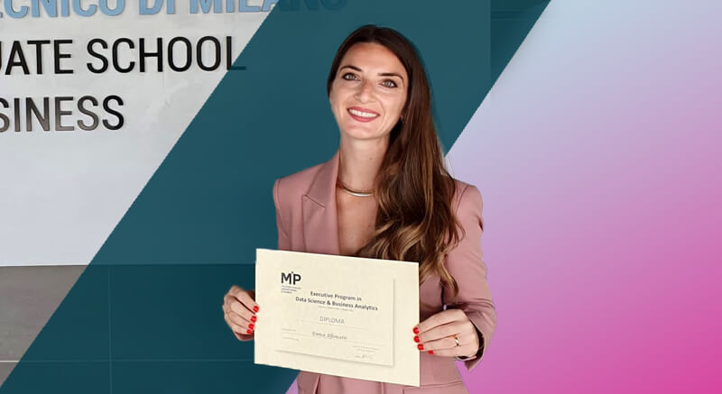
Continuous Improvement: Meet Enrica, Industrial Engineer
Find out how Enrica is advancing her career at prestigious universities around the world with tuition assistance from Boeing.
-
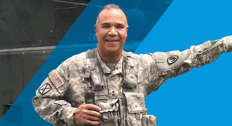
Leading by Example: Meet Tony, Vice President of Army Systems
Anthony 'Tony' Crutchfield, Boeing vice president and retired lieutenant general, shares decades of leadership experience with students and early career professionals from underrepresented communities.
-
Angelie Vincent, Product Development Engineer, Recounts Her Journey With Autism
Angelie has been with Boeing for 12 years and was diagnosed with autism in April 2019. Through her story, she inspires others to overcome adversity.
-
Meet Nathan: Phantom Works Operations Analyst
Nathan helps our defence customers make decisions using the power of modelling and simulation.
-
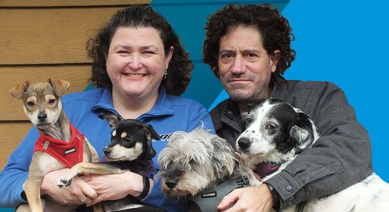
A Mother-Daughter Duo Bond Over Invention
Meet Kay and Denise, inventors of an adhesive removal tool and an inspiration to other innovators across our company.
-
Accessibility Accommodations
If you need a reasonable accommodation for any part of the employment process, please contact us.
-
From mechanic to manager
Read how our leadership training helped Jacob hone his management skills and grow his career.
-
It’s No Ordinary 9 to 5 For Manufacturing Engineer Lee
Meet Lee, a manufacturing engineer in Boeing’s Melbourne factory who has worked on commercial and defense aircraft, including the first Australian-made autonomous military aircraft, known as the MQ28A Ghost Bat.
-
We never stop growing
Whether you’re looking to expand your knowledge or grow as a leader, our development programs are designed to help you succeed.
-
'What are your qualifications?'
Meet Danielle and Ankita, two teammates who are breaking biases with the help of allies.
-
Cyber Security Guard: Meet Anna Guthrie, Product Security Engineer
Product security engineer Anna Guthrie builds resilient technologies to protect against cyberattacks. In this interview, she offers a glimpse into a day in her life with our growing cybersecurity team.
-
No barriers to entry
Three teammates champion a new approach to helping overcome the “mid-career crisis” and increasing diversity at all levels.
-
Unlock the secret to conquering fear
Engineering manager Aslihan Karlidag uses Boeing’s digital learning opportunities to keep her fears at bay
-
“There’s no better place to explore new roles and opportunities than Boeing.”
Chad, a Senior Software Manager, knows that growth happens outside the comfort zone.
-
‘When you feel like the professor, it’s time to be the student again’
Vice president Tresha Lacaux landed her dream internship at Boeing. Today, she’s landed her dream role
-
-
'I feel a part of the Boeing family'
Discover how our Neurodiversity at Work program helped Thomas launch his software engineering career.
-
‘I’m inspired by the belief that we can always improve’
Meet Dr. Rongsheng “Ken” Li, a Principal Technical Fellow who has been awarded for his work in aerospace guidance, navigation and control systems.
-
Meet Suba, a Space Launch Systems Leader who Broke Barriers
Discover how Suba Iyer turned her fascination with how things work into an engineering career.
-
From Interns to Innovators: Systems Engineers Blaze Paths to Success
Meet two systems engineers who are contributing to the next era of spaceflight.
-
Meet Sanh, 777X Design Engineer
Read how Sanh Ha, an engineer who is deaf, applied innovative thinking to safely overcome obstacles during a test flight.
-
'We are finding ways to inspire more people around us'
Meet Nic, a leader in the UK who is advancing equity and entrepreneurial innovation to solve aerospace challenges.
-
From Making Soap to Making a Difference: Meet Oscar Johnson
A lifelong interest in chemistry sparked this engineer to desegregate lunch counters in 1960 and unveil cutting-edge technology in Boeing laboratories 50 years later.
-
'There's room for all types of leaders'
Meet Teresa, a product engineer and inventor with multiple patents.
-
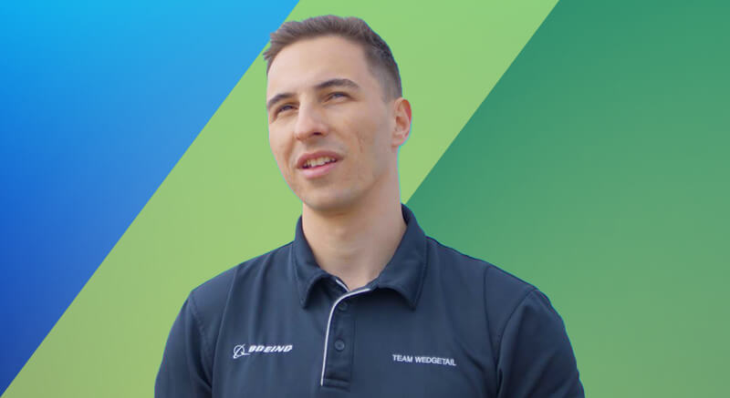
Meet Bo, E-7A Wedgetail Systems Engineer
Bo designs and develops software and hardware that supports the Wedgetail's missions. Watch the video to learn how his work has an immediate impact.
-
Recruitment Fraud Alert
Be aware of fraudulent job offers purporting to be from The Boeing Company and/or its affiliates. Learn what to look for.
-
Meet Marvi Matos Rodriguez, Design Practices Engineer
Marvi applies her love of invention to challenging problems, and works towards her personal mission: to serve as many people as possible.
-
Meet Nelson Akwari
Read about Nelson's journey from the soccer field to becoming an accomplished engineer and leader at Boeing South Carolina.
-
Keeping the World Moving
Meet Susana, a supplier quality specialist in Mexico who's using problem-solving skills to drive operational excellence.
-
Easing the Transition of U.S. Service Members
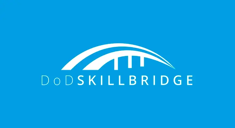
Learn how our partnership with SkillBridge is supporting veteran teammates in discovering their next mission.
-
-
Meet Jacqueline Lam, Global Sustainability Leader
An inclusive approach is helping Jacqueline drive sustainable aviation in Southeast Asia.
-
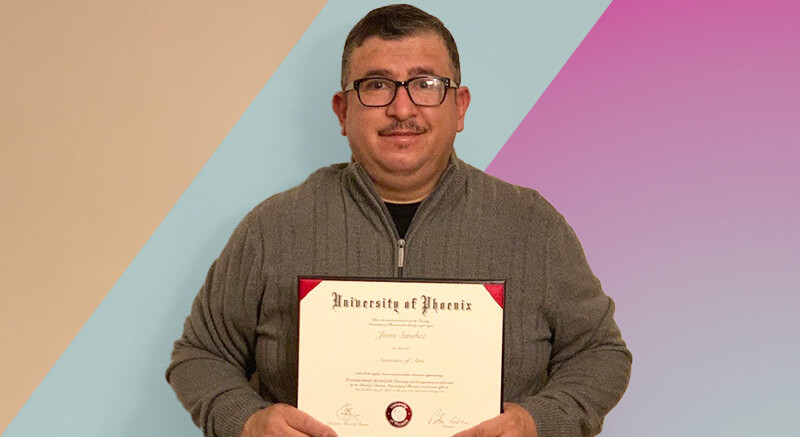
Clocking In: How 7 Hours a Week Changed Jesus’ Life
Meet Jesus Sanchez, a power machine operator in Auburn, Wash. See how Jesus used our tuition assistance program to obtain an associate degree in business.
-
Three Keys to Mission Success
Alex Campos, a Boeing Missile Defense contracts administrator and U.S. Navy reservist, shares his advice for staying on mission.
-
Building a Family On Their Terms
Read how Kristin Innes and her partner Bonnie are growing their family with help from Boeing's fertility benefits.
-
Not Your Ordinary 9 to 5
Meet Jimmy, an Air Force veteran and aviation safety coordinator that helps teams operating the F/A-18F Super Hornet and EA-18G Growler get home safely.
-
‘If you do right, right will follow you’
Engineers Debra and Stacia discuss the importance of community connection and making an impact through even small actions.
-
Meet KJ
From the Rosebud Reservation in South Dakota to leading attack helicopter programs in Mesa, AZ., Kathleen “KJ” Jolivette inspires STEM interest among Native American students.
-
'It's hard to describe the thrill of it'
Meet Ty'Quish, a mechanical engineer who has helped design and build the next-generation assault helicopter.
-
Meet Jinnah Hosein, Vice President and Chief Software Engineer
Our software engineering challenges are immense. But the possibilities are even greater. Learn how our team is harnessing the power of future-forward computing.
-
An Engineer's Creative Edge Helps Customers Chart Their Course
A a modeling and simulation engineer for Boeing Ground-based Midcourse Defense, or GMD, Kyle mostly deals in a world that’s conceptual, using a modeling system to simulate and predict how a customer request will perform in a real-world scenario.
-
It's a learner's paradise: Meet Rakesh Nanda
Discover how Rakesh and the design engineering team at the 787 Interiors Responsibility Center in India innovate and grow.
-
The Best Call That I've Made
Faced with caring for two sick family members, Sandra Lankford leaned on Boeing's caregiver benefits for support. Watch Sandra's story.
-
Automation is the Future
Read how Sarah Wauahdooah, a manufacturing research and development engineer, applies her robotics expertise on the V-22 Osprey program.
-
Meet Satyaki, Helicopter Engineer
Satyaki helps to keep the Australian Army’s CH-47 Chinook helicopters flying around the clock.
-
‘I gained a family of leaders’
Stephanie Yount, engineer and recent Leadership Next graduate, discovers she’s most comfortable when she’s completely uncomfortable.
-
'You can have 20 careers at Boeing'
Meet Boeing finance leader Terrence Chance, and discover the breadth of the experience that's shaped his career.
-
UK Equal Opportunity Statement
We are an equal opportunity employer.
-
Non US EOE Statement
We are an equal opportunity employer.
-
5 Tips for Acing Your Virtual Interview
Dalena Nguyen, a Talent Acquisition Advisor, shares her top tips for making a great first impression when interviewing by phone or online.
-
'Never stop learning'
Discover how our digital learning resources helped Boeing India teammate Antara upskill.
-
Meet Abbey Carlson: Former Intern Turned Space and Launch Engineer
Abbey Carlson, a former Boeing intern, shares her two major milestones: graduating from college and accepting her first job with Boeing.
-
Meet Francis: Inventor Strives to Make Space Safer
A Senior Composite Engineer at Boeing’s Satellite Development Center, Francis, says each patent represents a step toward achieving her childhood goal to make space safer.
-
‘Engineering reaches every industry; it’s part of everyday life’
Meet Hana McKee, an engineer whose curiosity inspires her to innovate the next generation of rotorcraft.
-
Jae’s Early Fascination With Flight Led to a Role at Boeing
Meet Jae, a systems engineer on the world’s leading airborne early warning and control aircraft, Boeing’s E-7A Wedgetail.
-
A Veteran's Secret Weapon
What Marcie Purser, program management specialist, brings to the table is highly valued at Boeing: lasting connection.
-
On a Mission to Lead
Learn how one of our development programs – a partnership with MIT – is helping an engineer get on a path to executive leadership.
-
'The possibilities are endless'
From space to defense, senior software and project engineer, Kimberly Sledge, inspires the next generation of Black women in STEM.
-
Meet OB, Starliner Spacecraft Technician
From making repairs on aircraft to building spacecraft, Oborsouis "OB" has had his hands in a little bit of everything.
-
Aim High: Meet Kristine, Space Launch Systems Engineer
Kristine Ramos, design engineer, goes above and beyond to advocate for human spaceflight.
-
‘I’m a lifelong learner’
Meet Nixon, an engineer who uses our tuition assistance to stay on the cutting edge of emerging technology.
-
‘I don’t just translate — I bridge gaps’
Meet Dama, an engineer and manager who strengthens our company by being a cultural and technical integrator.
-
‘I’ve challenged myself to grow’
Read how Kaomi Hashimoto has grown her career across continents, while supporting our next generation of leaders.
-
'Helping people reach their potential inspires me'
Meet Wilton, a Quality manager for the Space Launch System program who helps create a culture where everyone can speak up.
-
‘I encourage others to take this opportunity!’
From aircraft assembler to avionics engineer, Vadym Vasylyshyn grew his career with our tuition assistance program.
-
'Lean into discomfort': Career Advice From a Chief Engineer
Pete Kunz, Phantom Works chief engineer, describes opportunities that have shaped his career and shares tips for success.
-
'It may not be easy, but it will pay off': Meet Rayni Sivley
As project manager for Ground-based Midcourse Defense, Rayni isn't bothered by roadblocks. Read her advice for career growth.
-
Love at First Flight
An operations manager and an analyst for the V-22 tiltrotor thrive on teamwork in the factory and at home.
-
The sky’s the limit
Meet Ronak, a Boeing India teammate who’s used our tuition assistance to grow his career, studying online and abroad.
-
-
Excellence with Caring' is Key: Meet Dr. Nathan Brooks
Boeing's first Black Senior Technical Fellow grew from humble beginnings to executive leader and mentor.
-
AI creator changes how autonomous systems work
‘It’s about technology and innovation that will transform aerospace as we know it.’
-
-
-
Explore careers with Boeing Phantom Works
Discover a career with Phantom Works, Boeing’s advanced research and development division, and shape the future of aerospace. Apply today for engineering, cybersecurity, data intelligence jobs and more.
-
Jenna’s career path has been anything but traditional.
Veteran, military spouse and engineer, Jenna believes there are many paths to success.
-
-
-
“When you ask veterans for help, you get it.”
Joshua, a veteran of the U.S. Air Force, once helped repair our aircraft. Now he flies in them.
-
-
-
Tristan Crumley | Design Engineer Intern
Tristan helps his team create experimental hardware designs for propulsion applications.
-
Adrian Sosa | Structures Design Engineer Intern
Adrian supports the efficiency and reliability of 777X wing structures through innovative design solutions.
-
Mya Beathley | Engineering Intern
Learn how Mya contributes to safety and certification standards for Boeing Defense, Space & Security.
-
Eva Strang | Strategy Analyst Intern
Through Aerospace Xelerated, Eva supports aerospace startups, fostering innovation and industry advancement.
-
Elisa Rwagasana Ishimwe | Information Technology and Data Analytics Intern
Elisa’s passion for aviation motivates her to enhance internal tools that improve collaboration.
-
Niyathi Gorantla | Sustainability Intern
Meet Niyathi, who manages projects for our Sustainable Aerospace Together Forum.
-
-
Atira Sarat | Sustainability Innovation Research Intern
As a Research Intern, Atira is working on real-world projects and helping to shape the future of aerospace.
-
Adrian Loekman | Airplane Maintenance Engineering Intern
From day one, Adrian felt welcomed and part of a collaborative team.
-
Đoàn Sĩ Anh | Retrofit Engineering Intern
From Vietnam to the United States, Doan learned about our company from engineers around the world.
-
-
A passion for propulsion helps fuel the future of flight
Dominic and his team are at the forefront of studying alternative energy sources and future flight concepts.
-
Learn how having a security clearance can open new career and growth opportunities in the aerospace and defense industry
-
Security clearance levels for aerospace & defense jobs explained
Learn about the different security clearance levels required for aerospace and defense jobs. Learn how to transfer active clearances to a job at Boeing
-
High-demand jobs for people with security clearances
Learn how having a security clearance can open new career and growth opportunities in the aerospace and defense industry.
-
Two Ways To Stay Connected
Join our Global Talent Network and sign up for Job Alerts to learn about additional opportunities.
-
Benefits
Our Total Rewards program includes best-in-class benefits designed to meet your needs at every stage in life.
-
Working Here
We're a company of inquisitive, talented people. Find out what's important to us and what inspires us to do amazing things together.
-
Inside Boeing
See what it means to be part of #TeamBoeing. Explore stories and learn how our people grow their careers while shaping the future of aerospace.
-
Our Locations
Our global presence includes employees and operations in more than 65 countries. Explore some of our locations.
-
Frequently Asked Questions
See some of the most commonly asked questions about starting a career with Boeing.
-
Search for Events in Your Area
Our hiring events are a great way to learn about our innovations and culture.
-
Military and Veterans
You can join the more than 18,000 veterans who chose Boeing to be their next mission.
-
Entry-Level Careers
Work on projects with a scope few companies can match in an entry-level role — where many of our senior leaders started their careers.
-
Internships
Gain hands-on experience and work alongside a team of industry leaders as you help build the future.
-
-
-
Manufacturing and Quality Roles in Seattle
Build advanced aerospace products while growing your skills and earning best-in-class benefits.
-
Boeing in South Korea
We’re proud of our 75-year partnership with South Korea. Join us and help revolutionize aerospace development from the heart of Seoul.
-
Boeing in India
The most exciting advances in aerospace are being developed today in India. Join us and build a career at the center of our industry’s future.
-
Boeing in the UK
Across 30 key locations in the UK, we employ more than 3,000 highly skilled teammates. And, after 80 years of success, we keep growing.
-
Boeing in Washington, D.C.
Whether you're a software engineer, systems engineer, or cyber analyst, help us solve tough challenges and contribute to the security of the nation.
-
Boeing in Missouri
Join us and contribute to next-generation aircraft, training, and defense products and capabilities.
-
Boeing in Poland
We develop technologies that will shape the future of flight and we need your curiosity and unique perspective to help keep us innovating.
-
Boeing in Oklahoma
Learn how we continue to create opportunities for bright minds and see what makes this a great place to build a career.
-
Boeing in Alabama
As the largest aerospace company in the state, we play a vital role in the U.S. space and defense programs.
-
Boeing in California
As we transform aerospace, your skills will take center stage. Join us and help connect, protect and explore our world and beyond.
-
Boeing in Brazil
For more than 90 years, we’ve partnered with Brazil and today you can join a team filled with creative minds who are building what’s next.
-
Boeing in Texas
Explore what makes Boeing in Texas a great place to work.
-
Boeing in Japan
For more than 50 years, we’ve worked closely with Japan to help create the future of aerospace and bring new expertise to our future-focused products.
-
Boeing in Arizona
Known for producing the Apache and Little Bird aircraft, we’re also home to centers of excellence in software, composites, wiring and fabrication.
-
Boeing in South Carolina
Across our manufacturing plants, research and technology center, engineering center and propulsion sites, we’re developing new advances in flight.
-
Boeing in Washington State
At the center of aviation since 1916, many of our most innovative products are designed and built here.
-
Cybersecurity Careers at Boeing
Boeing is more than airplanes. More than satellites. More than cutting-edge cyber solutions. We work together with advanced technology on projects for the defense and intelligence communities. Join our Cybersecurity team.
-
Electronic and Electrical Engineering Careers at Boeing
Electrical engineers work closely with our customers to develop electronic and electrical systems for Boeing aircraft, and world-class autonomous robotic systems for space, terrestrial, and underwater hardware. Learn more about the team.
-
Finance Careers at Boeing
Our finance professionals play a key role in guiding critical business decisions and cutting-edge solutions for the world’s leading aerospace company. Learn more.
-
Flight Engineering Careers at Boeing
Flight engineers are essential to the development, safety and success of our products and solutions. Learn more about the team.
-
Information Technology Internships at Boeing
Learn how you can get access to cutting-edge technology and grow your skills through our Information Technology & Data Analytics Intern Program.
-
Electrical Engineering Internships
A chance to start your career designing and building our next generation of products.
-
Human Resources Careers at Boeing
Boeing HR professionals support our employees as they manage their career path, develop their teams and chart the course for career development. Learn how you can join the team.
-
Industrial Engineering Careers at Boeing
Discover how you can make a difference at Boeing as an industrial engineer. Become part of a team that drives innovation across diverse technologies worldwide.
-
Test and Evaluation Engineering Careers at Boeing
As a Test and Evaluation Engineer at Boeing, you'll ensure that our next-generation commercial and defense products and systems meet the highest standards. Join us as we continue to push the boundaries of aerospace.
-
Software Engineering Careers at Boeing
As a software engineer at Boeing your code will power products that defy gravity and fly faster than the speed of sound.
-
Supply Chain Management Careers at Boeing
With a career in supplier management at Boeing, you can help solve business challenges that are redefining an entire industry.
-
Systems Engineering Careers at Boeing
As a Systems Engineer at Boeing, you can help drive the overall design of innovative and high-quality products and solutions.
-
Business Operations Internships
In our Business Intern Program, you can be part of a team that is helping shape the future of aerospace.
-
-
Human Resources Internships
In our Business Intern Program, you can be part of a team that is helping shape the future of aerospace.
-
Supply Chain Internships
In our Supply Chain Intern Program, you can be part of a team that is helping shape the future of aerospace.
-
Data Science and Analytics Careers at Boeing
Data doesn’t work in silos — it needs to breathe and interact with other information in order to tell the whole story, not just parts of it. At Boeing, we’re working across our enterprise to let data and information drive our collective decision-making. Join our Data Science and Analytics team today.
-
Information Technology Careers at Boeing
As part of our Information Technology and Data Analytics team, you’ll support one of the largest corporate IT portfolios anywhere. Join us and help build the future.
-
Materials, Process and Physics Engineering Careers at Boeing
Come build the future with Boeing and develop the next generation of aircraft, space and underwater vehicles and revolutionary approaches to manufacturing.
-
Mechanical and Structural Engineering Careers at Boeing
Mechanical and structural engineers at Boeing develop and apply innovative technologies that shape the future. Learn more.
-
Product Security Engineering Careers at Boeing
Discover how you can make a difference at Boeing as a product security engineer. Become part of a team that drives innovation across diverse technologies worldwide.
-
Production Engineering Careers at Boeing
At Boeing, our production engineers use their skills to build the future of advanced manufacturing. Learn more.
-
Manufacturing Careers
Every day around the globe, Boeing manufacturing employees build the future of aerospace. Join our team. Your future is waiting.
-
Specialty Engineering Internships
A chance to start your career designing and building our next generation of products.
-
Software Engineering Internships
A chance to start your career designing and building our next generation of products.
-
Systems Engineering Internships
A chance to start your career designing and building our next generation of products.
-
Test & Evaluation Engineering Internships
A chance to start your career designing and building our next generation of products.
-
-
-
Global Real Estate and Facilities Internships
A chance to start your career designing and building our next generation of products.
-
Finance Internships
In our Finance Intern Program, you can be part of a team that is helping shape the future of aerospace.
-
Flight Engineering Internships
A chance to start your career designing and building our next generation of products.
-
Industrial Engineering Internships
A chance to start your career designing and building our next generation of products.
-
Materials, Process & Physics Engineering Internships
A chance to start your career designing and building our next generation of products.
-
Mechanical & Structural Internships
A chance to start your career designing and building our next generation of products.
-
Facilities and Asset Management Engineering Internships
A chance to start your career designing and building our next generation of products.
-
Boeing in Ukraine
Our teams in Ukraine provide engineering expertise, consultation services, research and technical assistance for our platforms and aircraft that fly worldwide.
-
Boeing in Australia
Join a team of more than 4,300 people providing leading-edge aviation services for our defense and commercial customers.
-
Product Support Engineering Internships
A chance to start your career designing and building our next generation of products.
-
Product Security Engineering Internships
A chance to start your career designing and building our next generation of products.
-
Production Engineering Internships
A chance to start your career designing and building our next generation of products.
-
Safety & Airworthiness Engineering Internships
A chance to start your career designing and building our next generation of products.
-
FAQs on applying for jobs that require a security clearance.
Find answers to common questions about applying for aerospace and defense jobs that require a security clearance.
-
Career development for military spouses at Boeing
Explore job opportunities for military spouses at Boeing, including for jobs that require security clearance.
-
-
From excavating bones to building Boeing systems
Tori started her career digging up ancient bones as a budding archeologist. Today, she’s a systems engineer for our E-7A Wedgetail program in Adelaide, South Australia.


Jobs for You:
No recently viewed jobs.
View all of our available opportunitiesNo saved jobs.
View all of our available opportunitiesConnect with us
Join our Talent Community
Get updates about Boeing job opportunities, events and career information.
Sign up for our Talent CommunityVeteran Talent Community
Transition to a career in engineering, product support, IT, manufacturing or other areas.
Sign up for our Veteran Talent Community